A Spike based ADC for calcium bio-signal recording in the mouse brain

We designed and developed a neuromorphic VLSI device which comprises a bio-signal recording amplifier with a spike based analog to digital converter (ADC) for optical recording setups. The purpose of the ADC is to digitize a fluorescence signal from calcium imaging in mice brain. The signal is transmitted on a photodiode via optical fibers. The advantage of a neuromorphic ADC compared to the classical recording system with a CCD camera is a much higher bandwidth and a lower power consumption. As biologists are often interested in a temporal signal difference between two recording channels in the range of milliseconds, this project might lead to novel useful results.
The ADC circuit implemented on the chip is based on the silicon retina pixel described in [1]. It consists of a logarithmic photo-detector, two amplifiers and two self-timed circuits that compare the amplified voltage to a threshold and produce an event and reset when the threshold is reached. In this way a change in input is encoded as the time difference between two events (delta modulator). It has a power consumption of 11μW , uses an area of 3100 μm 2 and it can process input signals with a bandwidth of 11m to 1.1 kHz. These features make the circuit attractive for recording applications directly on the animals or brain computer interfaces.
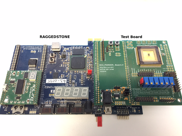
We already showed with circuit simulations that the ADC is able to encode the fluorescence input signal precisely enough to allow a faithful reconstruction. In this project the student will characterize the real circuit, using an optical bench and well controlled signal sources. You will learn how to work with an optical bench and with boards that interface the full-custom chip with Field Programmable Gate Array (FPGA), required to get input signals from the device. Since as light source we will use a laser beam, it will be necessary to properly align the photosensitive area of the chip with the laser beam, while shielding the other light-sensitive circuits on the chip.
The chip characterization will require also the programming of the FPGA, which will be used to send input signals to the chip and to collect output events in response to the light-modulated stimuli, and to analyze the quality of the signal reconstruction.
The project is a short project, but can be extended to include measurements from a real optical-recording experiment, with our colleagues from the lab of Prof. Firtjof Helmchen. You will learn how optical fibers work and you have the opportunity to collaborate with HIFO to apply the setup to bio-signal recording experiments.
Contact
For more details, please contact Giacomo Indiveri (giacomo (at) ini.uzh.ch)